Scanning Electron Microscopy Analysis for Automotive Failure Investigation
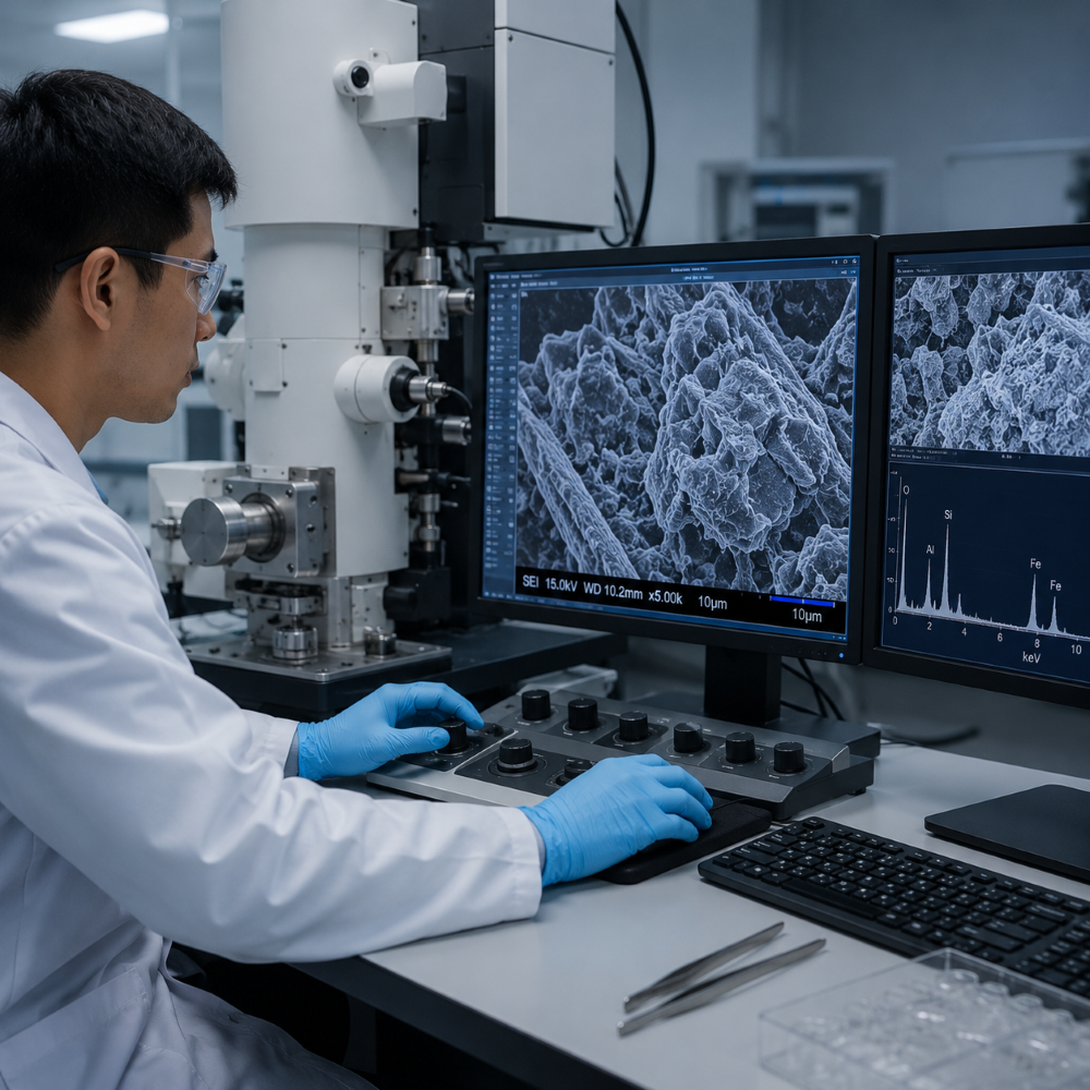
Not every automotive failure shows its full story under a regular microscope. A cracked component might only reveal a small fracture line, while the real explanation is hiding in surface features, corrosion buildup, coating layers, or a stray particle that’s too small to see clearly with normal optical equipment. Scanning electron microscopy analysis uses a focused electron beam instead of light to image a sample at much higher magnification, and when paired with EDX, it can also identify what a particle or deposit is actually made of.
What SEM Actually Shows You
An SEM scans an electron beam across the sample and picks up signals from how the beam interacts with the material. Secondary electron imaging is the most common mode, and it’s great at showing surface shape and texture, things like fracture faces, corrosion pits, or the outline of a particle. Backscattered electron imaging works a bit differently. It highlights compositional differences, so areas with heavier elements show up brighter than areas with lighter ones.
This makes SEM useful for fine cracks, coating defects, or particles too small to judge with the naked eye.
SEM Imaging and SEM-EDX Aren’t the Same Thing
SEM imaging on its own shows shape, texture, and how a feature sits relative to the surrounding material. That’s often enough to tell a fatigue fracture apart from a ductile overload, or to figure out whether corrosion started at a pit, an interface, or a weak spot in a coating. SEM-EDX goes a step further by reading the X-rays the sample gives off under the beam, which tells you which elements are actually present.
| Method | What it shows | Typical use |
| Secondary electron imaging | Surface shape and texture | Fracture features, corrosion pits, particle shape |
| Backscattered electron imaging | Compositional contrast | Alloy phases, inclusions, coating differences |
| EDX point analysis | Elements at one specific spot | Identifying a particle or deposit |
| EDX elemental mapping | Where elements are spread across an area | Coatings, contamination, segregation |
Worth knowing: EDX has limits. It might tell you a deposit contains carbon and oxygen without telling you whether that organic material is epoxy, polyester, or something else. When the molecule itself matters, a technique like FTIR usually has to step in.
Where This Shows Up in Automotive Investigations
Fracture and fatigue analysis is probably the most common use. Features like fatigue striations, cleavage facets, and microscopic dimples on a broken surface tell investigators roughly how and where a crack started. Corrosion investigations lean on SEM to look at pit shape, crack paths, and the deposits sitting on a corroded surface, with EDX backing that up by identifying what those deposits actually contain.
SEM also comes up a lot in particle identification, whether that’s debris from hydraulic systems, contamination on electrical contacts, or particles pulled off a cleanliness-testing filter. Combining shape with elemental makeup helps investigators tell machining debris apart from mineral contamination or stray fibers. Beyond that, it’s regularly used for coating cross-sections, surface treatment checks, solder joint inspection, and PCB failure analysis.
SEM vs Optical Microscopy
Optical microscopy is still useful for a quick first look since it covers larger areas fast and shows color, but it hits a resolution wall pretty quickly. SEM goes further, offering sharper detail, better depth of field, and the option to pair imaging with elemental analysis.
| Point of comparison | Optical microscopy | SEM analysis |
| Image source | Visible light | Electron beam |
| Best for | Larger visible features | Micro and nano-scale features |
| Depth of field | Lower on rough surfaces | High |
| Elemental ID | Not available | Available via EDX |
| Best used for | Initial inspection | Detailed root-cause analysis |
In practice, the two aren’t competing tools. Optical microscopy usually finds the area worth a closer look, and SEM takes it from there.
Getting Sample Prep Right
Metal and ceramic samples often need little prep if the surface is already clean and fits the sample chamber. Softer, non-conductive materials like polymers or rubber usually need a thin conductive coating first to stop the image from distorting under the beam. Cross-section work takes more effort. The sample may need cutting, resin mounting, grinding, and polishing to expose internal layers or cracks, and careless handling at this stage can wreck the very features the analysis is supposed to reveal.
When to Bring In SEM Analysis
SEM is worth considering once visual inspection and a regular microscope can’t explain why a part failed, what a particle is, or where a coating problem began. It helps to give the lab background details up front, things like the component material, service conditions, where the failure showed up, and the specific question the investigation needs to answer.
Companies that need scanning electron microscopy analysis for fracture investigation, corrosion characterization, contaminant identification, or coating analysis can work with ALS Testing, which carries out this work under an ISO/IEC 17025:2017 accredited system. ALS Testing also supports manufacturers and engineering teams with failure analysis projects in Malaysia, providing SEM investigations for automotive, electronics, and industrial applications where detailed root-cause evidence is required. The most useful SEM investigation isn’t the one run at the highest possible magnification. It’s the one built around a clear question, proper sample prep, and results that actually hold up to engineering review.